Operating System Realization for Real-Time Visualization of CAN-Bus Data Streams using Xilinx Zync SoC
on
Journal of Electrical, Electronics and Informatics, p-ISSN: 2549–8304 e-ISSN: 2622–0393
44
Operating System Realization for Real-Time Visualization of CAN-Bus Data Streams using Xilinx ZyncSoC
Mohammad J.M Zedan
Computer and Information Department College of Electronics Engineering/ Ninevah University Mosul, Iraq
mohammad.jassim@uoninevah.edu.iq
Abstract The revolution in the automotive industry over time led to more and more electronics to be included in the vehicle and this increased the number and space allocated for cables. Therefore, the in-vehicle cabling network has been replaced with a two-wire bus serial communications protocol called Controller Area Network (CAN). The proposed paper described the implementation of the CAN controller as a listener to monitor the state of the CAN bus in a real-time approach. The CAN listener obtains the data from the CAN bus by using an external signals converter. The work was realized using development platform called ZedBoard. The controller performed a sequence of processes on the received CAN frames including decoding, buffering and filtering. The processed data was stored in an implemented FIFO to keep the data from loss. After that, the data was sent serially to the processor system over the implemented SPI that connects the controller with the processor of the Zynq-7000 device. A single-threaded, simple operating system was run over the processor to provide a set of libraries and drivers that were utilized to access specific processor functions. It enabled the execution of the C code that was written to configure the operation of the onboard display unit. The design procedure and simulation process for the implemented CAN listener was achieved using the Xilinx ISE WebPACK environment, while the final complete design was properly tested and verified by connecting the module to a CAN network consisting of six CAN nodes.
Index Terms—CAN, SoC, ZedBoard, FIFO, ISE WebPACK.
The Controller Area Network is an asynchronous bus network that defines a standard protocol for effective and reliable serial communication between devices, sensors, and actuators for real-time control applications[1]. The CAN network uses the bus topology, in which every node in the network is connected to other nodes without using a central controller for the entire network. The CAN controller specifies the bus level by the potential difference between two wires that comprise the CAN bus. The CAN protocol introduces two logical states: dominant and recessive levels which are identified as a logic ‘0’ and logic ‘1’ respectively. The transmitting node can broadcast a message to all the receiver nodes by changing this bus level [2, 3].
The CAN bus has a maximum data rate of up to 1 Mbit/s for a maximum distance of 40 meters. CAN protocol use broadcast communication technique (Multi-master bus) in which every node can send messages to all other nodes on the bus and each node selects the interesting messages using filters and responds only to wanted messages. The CAN bus provides a very high level of security, sophisticated error detection and correction techniques with assumptions of no data can be lost [4, 5].
The interest in CAN protocol has increased recently due to the large number of applications that use it and also the availability of the robust mix of on-board peripherals and expansion capabilities of ZedBoard, all these give an incentive to implement this important protocol on this integrated platform.
The objective of this work is to implement a CAN listener on ZedBoard using an operating system running on the Zynq processor[6]. The Register Transfer Level (RTL) model of the CAN controller was developed using a general-purpose parallel programming language called VHSIC Hardware Description Language (VHDL) and the functional simulation
of the model was obtained. The complete design for the controller was divided into twelve sub-modules where each one performs a special function. These sub-modules were integrated to work as a single unit to implement the CAN listener module. To configure the functions of the Zynq processor under the stand alone operating system, a C code is also written in an Object-Oriented manner. The final design of the CAN listener module was tested by connecting the module to an actual CAN network.
The vital problem being addressed was the design and improvement of a one-chip solution for a CAN controller as a listener using the ZedBoard platform. As a listener, the CAN controller should not send any frame to the CAN network. The CAN listener acquires the data from the CAN bus by connecting the transceiver adapter directly to the board. The transceiver converts the differential signals from the network to digital signals. When data is received, it is necessary to decode the different data input streams and to realize specific protocol mechanisms like message buffering and filtering. After that, the processed data should be sent to the processor using one of the serial communication standards like Serial Peripheral Interface (SPI). Finally, the data streams should be displayed using the onboard display unit called OLED which is connected to the processor.
An introduction to the CAN listener is given in Section I. Section II presents the related work. Sections III, IV and V show the building blocks of the developed CAN controller. The results, performance analysis, and the actual test explained in sections VI. Finally, section VII concludes this paper.
-
II. LITERATURE REVIEWS
A lot of attempts for monitoring the CAN bus have been made; for instance, the works in [7],[8] and [9] described the design, simulation and FPGA implementation of a protocol controller for the CAN 2.0. It also deals with the design process of the FPGA, coding, simulating, testing, and finally
programming the FPGA. The RTL based design of the CAN controller was implemented using Verilog HDL.
A LabVIEW in [10] was used to compile a CAN bus monitor system. It abstracted the signals data from data frames transited in the CAN bus. A computer, plug-in hardware, and Lab VIEW comprised a completely configurable virtual instrument to accomplish tasks. A National Instruments™ CAN-board (NI-CAN) was used to interface a CAN bus in this system.
The authors in [11] employed a 32-bit ARM Cortex-M series microcontroller with its on-chip CAN and USB peripherals were used to implement a USB-CAN adapter and custom firmware that could be ported on a variety of boards provided with these two communication interfaces. The host PC runs a GUI developed using standard DLL libraries provided by the host Windows operating system to demonstrate the CAN-USB gateway.
Gong, S., et al[12], proposed the use of the reusable IP(Intellectual Property) technology in FPGA as the core controller. Also, the CAN communication system was implemented by System-on-a-Programmable-Chip (SOPC) technology. The MicroBlaze soft-core was used as an embedded processor in FPGA. The AXI Quad SPI core was used to implement the SPI control logic and the AXI INTC core to implement the interrupt control. MCP2515 and PCA82C250 were used to realize message transmission and reception in hardware design.
In [13] a Real-time Data-logger was designed for diagnostics display. Data acquisition from the bus was achieved using Arduino Uno R3 and MCP2515 CAN Bus Shield. Vector CANoe 9.0 was used for designing and simulating the CAN network. The data acquisition system is tested on this simulated network thus, acquired data is displayed on MATLAB GUI which can be used for fault detection and analysis.
Haoet al.[14]proposed to analyze the controller area network protocol in a way in which the Layered modeling method was adopted to build the CAN network model in the OPNET Modeler simulation environment. The models of Logical Link Control and Medium
Access Control of CAN protocol with the functions of error handling and channel status detection was established in the OPNET node Layer and the model of CAN bus physical layer was designed to implement collision detection and nondestructive arbitration functionality in the OPNET Pipeline Stages.
Presi T. [15] proposed the implementation of the CAN protocol using a PIC microcontroller for a vehicle monitoring system. Two PIC microcontrollers were used; both having the CAN protocol as a built-in device. The main feature of the system included monitoring of various vehicle parameters such as Temperature, presence of CO2 level in the exhaust and Battery Voltage. The software part was implemented in MPLab IDE using Embedded C, while the schematic was prepared using OrCAD.
It can be concluded from the previous studies that using microcontrollers integrated with CAN interface can degrade the performance, as the microcontroller is responsible for data communication (sending and receiving), in addition to reading inputs and driving outputs. This is a critical issue in industrial networks, where latency is a concern. In the case of using an individual CAN controller, there is a cost penalty as further IC is required, which increases the total cost for the implemented system. Finally, using the IP cores developed by FPGA
manufacturers and independent designers are usually not free of charge. All these factors evidence the need for developing a CAN controller module for smart sensors networking.
In this paper, the proposed work described the implementation of CAN controller as a listener to monitor and displayed the state of the CAN bus in a real-time approach for different standard bit rates. The controller was realized on the programmable logic of the ZedBoardplatform (SoC technology) using VHDL over the Xilinx ISE WebPACK environment.
The CAN listener controller had been realized on the
programmable logic of ZedBoard using the VHDL language. The design code was divided into a sequence of processes that were used for sequential statements to give a more powerful description of the design. These processes work concurrently to
perform the listening procedure. Fig. 1, shows the flowchart of
operations (processes) that performed on the received CAN
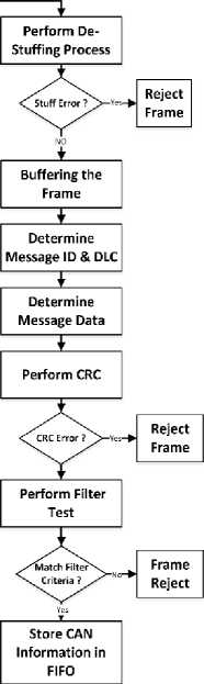
frames.
Fig. 1. CAN Listener Processes
The following is a brief description of all the processes that composes the CAN listener controller:
-
A. Baud Rate Prescaler(BRP)
All nodes on the CAN bus must use the same bit rate. As a result, the bit rate has to be calibrated for the different onboard oscillator clock frequency of the individual nodes in the CAN network[16].
ZedBoard supplied the Programmable Logic with four general-purpose clock outputs. A 32 MHz was used as a programmable clock source called (Crystal). This sub-module was used to create and adjust the CAN listener system clock (CLK) by dividing the on-board clock source (Crystal).
The CAN network could work with different standard bit rate as shown in the Table I. The bit rate of the CAN bus could be calculated using (1)[17]:
Bitrate =
Crystal (2 * N * Divisor)
(1)
Where N is an integer number that expresses the number of the fixed units called Time Quanta (TQ) that used to represent the bit time, where each TQ equals twice the oscillator period.
A register called Baud-Rate Prescaler (BRP) was used to assign values to the divisor. The BRP could be configured indirectly when the value of BRP is sent from the processor to the controller via the SPI.
TABLE I
BIT RATE RECOMMENDATION
|
Bit Rate (Kbps) |
NBT (µsec.) |
No. of TQ/bit |
TQ Freq.(MHz) |
BRP |
Divisor |
|
1000 |
1 |
16 |
16 |
“111” |
1 |
|
500 |
2 |
16 |
8 |
“110” |
2 |
|
250 |
4 |
16 |
4 |
“101” |
4 |
|
125 |
8 |
16 |
2 |
“100” |
8 |
|
100 |
10 |
16 |
1.6 |
“011” |
10 |
|
50 |
20 |
16 |
0.8 |
“010” |
20 |
|
40 |
25 |
16 |
0.64 |
“001” |
25 |
|
20 |
50 |
16 |
0.32 |
“000” |
50 |
-
B. Sampling and Synchronization Process
The CAN protocol utilized a Non-Return to Zero (NRZ) coding technique, which did not encode the clock inside the data stream; therefore, the CAN protocol used a complicated method of bit synchronization to compensate the phase shifts between the oscillator frequencies for all the nodes on the bus.
With this method, every node in the CAN network was incessantly resynchronized to make sure that all the nodes are synchronized at the same transmission rate (same nominal bit rate). The nominal bit rate was the number of bits per second transmitted without any resynchronization [17].
The nominal bit time (NBT) was the time required to transmit a single bit on the network and can be calculated using the inverse of the nominal bit rate.
The CAN bit time was comprised of four non-overlapping time segments. The Synchronization Segment (Sync_Seg) was the first segment in the nominal bit time and was utilized to synchronize nodes on the CAN bus. This segment had a fixed length (1) TQ. The transition of the bit was expected to occur within this segment. The second segment was the Propagation Time Segment (Prop-Seg), which was utilized for compensating the propagation delays of the signal across the CAN network. The length of this segment was between (1- 8) TQ[18].
Following the Prop-Seg,Phase Segment 1 (Phase_Seg l) was used for compensating the edge phase errors. The segment might lengthen during the resynchronization process. The final segment called Phase Segment 2 (Phase_Seg 2) was utilized also for compensating the edge phase errors. The segment might shorten during the resynchronization process. The length for each of the last two segments was between (1- 8) TQ [17].
The sample point was the point in the bit time located always at the end of Phase_Seg1 and it was used to read and to interpret the value of the current bit.
The sampling and synchronization processes were performed through reading the (RX_Trans) signal from the transceiver, which converted the on-bus differential signals to digital signals.
After that, every three consecutive values were stored in the temporary register called (RX_Reg). In case of the value of RX_Reg was equal to “110” or “001”, it means the transition
from logic ‘1’ (recessive) to logic ‘0’ (dominant) or from logic ‘0’ to logic ‘1’ has happened[19].
Every bit in the CAN listener module was represented by 16-time quanta. Thus, the sampling point should take place in a bit time number 13. A ring shift register of 16 bits called (TQ) was used to describe the time quanta module.
Only a single bit of TQ register was set to ‘1’ and this bit was shifted every time by one. Once the transition occurs, the bit was shifted obligatory to the bit location number 13 (sampling point). This procedure ensured synchronization for the whole design, whereas every bit (P) from the TQ register was used as a condition to coordinate all the processes that performed on the received CAN bit. When the sampling point was reached, the first value from the (RX_Reg) register was loaded to the (RX_CAN) signal which represented the input port for the CAN listener module.
-
C. Start of Frame Detection
Start of Frame (SOF) is a single dominant bit that indicates the beginning of the CAN frames. The main task for this bit is to synchronize all nodes on the CAN network after idle bus state.
In the CAN protocol, every two continuous frames were separated by Interframe Space which was composed of at least three recessive bits called the Intermission [17]. Following the Intermission, the bus remains in the idle state (recessive) until the beginning of the transmission for the nodes. At this time the detection of the dominant bit (SOF) on the bus was expected.
The detection process was performed by counting the number of recessive bits of bus idle state before the SOF bit. A counter called (Freecount) is utilized for this process. When the Freecount is greater than the intermission value, the first dominant bit that is received could be considered as the start for the new frame.
-
D. Bit De-stuff Process
Bit stuffing is the process of inserting non-information bits into the data stream in the transmitter’s side to improve synchronization and to provide signaling information to the receiver. On the receiver’s side, the de-stuffing process is performed to neglect the stuffed bit that is added previously.
As the SOF bit of the received message was detected, the de-stuffing process should be performed to delete the stuff bits before the extraction of the relevant information from the received message. To perform that for the CAN listener design, several states were used as described below:
-
• State (N) represented the new incoming value received from the bus.
-
• State (H1 – H5) represented the high-level (recessive) values.
-
• State (L1 – L5) represented the low-level (dominant) values.
-
• State (HS, LS) represented the high-level stuff bit and low-level stuff bit respectively.
-
• State (HE, LE) represented the high-level stuff error and low-level stuff error respectively.
In the CAN protocol, the de-stuffing process was only executed on a specific range called Destuff_Range (from the SOF bit until the end of the CRC field). Every newly received value located in the Destuff_Range was loaded sequentially to the N state and then it compared if its ‘0’ or ‘1’. In case the N state has ‘0’ for five consecutive states, it went from state L1 to L5.
After that, if the new bit comes ‘0’, the state went to LE (low-level stuff error), otherwise, it was going to HS (high-level stuff bit). Whenever a high-level value ‘1’ comes in between the five consecutive states, the state went directly to H1. The special case happened with the HS state (“000001”) when the state N comes ‘0’, the HS went to L1, otherwise, it goes to H2.
The same procedure was performed when the N state had ‘1’ for five consecutive states (H1 to H5). After that, if the new value comes ‘1’, the state went to HE (high-level stuff error), otherwise, it was going to LS (low-level stuff bit). When a low-level value ‘0’ comes in between the five consecutive states, the state goes directly to L1. Also, an exceptional case happens with the LS state (“111110”), when the state N comes ‘1’, the LS state goes to H1,otherwise, it goes to L2. The procedure that describes the de-stuffing process is shown in Fig. 2.
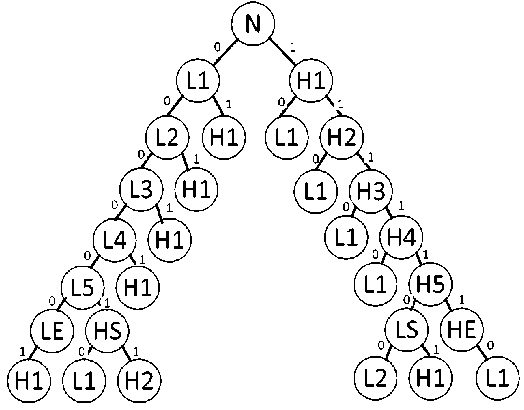
Fig. 2. The De-Stuff Procedure
To determine the validity of the received bit, a signal called RX_valid was used to specify if the received bit was data or stuff. This signal becomes ‘0’ only when there was high or low bit stuff (HS or LS). The other CAN listener processed work just in case the RX_valid is high. By using this procedure the stuff bit was omitted and the frame returned to its original value as before the staffing.
An error flag signal called Rx stufferr was set to ‘1’ in case of (LE or HE), to indicate that the received frame was incorrect. No error frames were sent back to the CAN bus because this controller works as a listener.
-
E. Buffering Process
After the SOF bit of the CAN frame has been noticed and the de-stuffing process has performed on the received bits, the clean frame should be loaded to a temporary buffer called (Message_Reg). The buffer was accessed constantly by every process in the CAN module to read the relevant data. This buffer must be cleared at the end of each frame and then should be reloaded with a fresh frame after the next receive.
-
F. Frame Types
The implemented CAN listener supported the standard data frames, extended data frames and remote frames (standard and extended). Neither error nor overload frames would be generated [20], since the controller worked as a listener. The type of received frame was determined by checking the IDE bit
and the RTR bit in the Message_Reg buffer. These bits had different locations, depended on the frame type.
When the IDE bit was ‘0’, it meant that the received frame was standard data frame; otherwise, the received frame was extended data frame. The same test was performed on the RTR bit to find out if the received frame is a remote frame or not. The remote frame could be standard or extended depending on the value of the IDE bit.
-
G. Message Identifiers
Every frame has a message identifier (ID) which is unique within the entire network. It located directly after the Start of Frame (SOF) bit. The ID defined the content and also the priority of the message that was utilized during the bus arbitration process when several stations compete for the bus access.
In this process, a special mask was used to extract the message identifier. Every time the mask was applied to the Message_Reg buffer to read the value of the message identifier for each frame. After that, the value of the identifier for the standard data frame which was 11 bits should be loaded to the (ID_Reg) register.
Once the extended data frame was received, an extra 18 bits should be loaded to the (EID_Reg) register which represents the extended identifier using the masking procedure. Accordingly, the total length for the identifier field became 29 bits.
-
H. Data Length Code
Data Length Code (DLC) is a 4-bit field indicates the number of bytes in the data field of the CAN frames [16]. The DLC field has different locations in the CAN frames depending on the value of the Identifier Extension (IDE) bit. Another mask was also utilized to take out the DLC value from the Message_Reg.
The acceptable values of the DLC field were zero to eight; point out, the data field contained data of zero to eight bytes length. If the value of the DLC field was bigger than eight then it was assumed that the frame includes eight bytes.
-
I. Message Data
One more mask was also applied to the Message_Reg buffer to read the actual CAN data from the data field and then loaded it to the (RX_Data). The length of the data field could be (0 - 8) byte depended on the value of the DLC register. The data field for the remote frame had no data, regardless of the DLC value.
-
J. Cyclic Redundancy Checker
Cyclic redundancy checking is a technique for detecting errors in the frames that have been transferred over a communication link. The transmitting node applied a fixed number of bits on a portion of the frame that was to be transmitted and then attached the resulting cyclic redundancy code on the CRC field of the frame and sent it.
The receiving node applied the same polynomial on the received data. If the receiving node noticed a mismatch between the calculated and the received data, the CRC error occurred and the message was rejected.
In the CAN listener module, the CRC value for every received frame was calculated by using a polynomial generator called CAN Polynomial which was represented in hexadecimal by 4599h [21]. The CRC procedure was performed on a special range of frame bits called (CRC_Range) which was started
from the SOF bit until the end of the data frame or until the end of the control field for the remote frame.
The bits that located in this range were divided by the polynomial specified by (2):
X15 + X14 + X1d + Xb + X7 + X4 + X3 +[21].(2)
The remainder of this division should be loaded to the (crcreg) register then it compared with the value of the CRC field which was part of the CAN frame. In case of mismatch is detected, the CRC result flag (CRC result) was set to logic ‘0’ (incorrect frame), otherwise, it set to logic ‘1’. This function was implemented using a 15-bit shift register and the exclusive or (XOR) to perform the dividing process.
Once the CRC_Range was ‘0’, the CRC process would do nothing; otherwise, the divisor was within the input (crcin). The divisor was then shifted by one bit, and the process was repeated until the divisor reaches the end of the input row.
-
K. Message Acceptance Filters and Masks
The main function of this module is to validate the incoming frames by checking the messages identifier (ID) to determine if the received frames are relevant to that particular node or not.
The acceptance filter was based on a special mask that was used to determine which bits in the identifier were tested with the filters. Table II described how each bit in the identifier was compared with the masks and filters to determine whether the message was accepted or not. If any mask bit was set to a zero, the corresponding bit would automatically be accepted, regardless of the filter bit [21].
TABLE II
FILTER AND MASK OPERATION [21]
|
Mask Bit |
Filter Bit |
Message-ID Bit |
Result |
|
0 |
X |
X |
Accept |
|
1 |
0 |
0 |
Accept |
|
1 |
0 |
1 |
Reject |
|
1 |
1 |
0 |
Reject |
|
1 |
1 |
1 |
Accept |
To control the reception operating modes for the valid frames, two bits called RXM were used. In case of the RXM were configured with”11”, it disabled the operation for the masks and the filters and the listener will receive any message on the bus.
When the RXM configured with”10”, only the messages with the extended identifiers would be accepted if they matched with the filter values. On the contrary, when the RXM equal to”01”, only the messages with the standard identifiers would be received when they matched with the filter values. Normally, the RXM bits were cleared to”00” to allow the reception of all the valid messages (standard or extended) as determined by the proper acceptance filters.
The CAN listener module had 13 registers that were used for the message acceptance operations. These registers must be loaded with the filters and the masks' values before the implementation process.
-
L. FIFO
The CAN listener should receive the frames from the CAN bus and perform all the processes in a real-time approach. A bottleneck happens in the final process when the listener
should display the processed information on the display unit which needs some delay. To solve this problem, a First In First Out (FIFO) was implemented to store and retrieve the processed data. This process prevented the loss of CAN frames information.
In the CAN listener module, the FIFO was built using a two-dimensional array called (fifo_store) where the numbers of rows (depth of FIFO) were 2048 and the numbers of columns (FIFO_width) were fixed to 96. Tow pointers were used to control the function of FIFO. The first one was called (writeptr) which increased by one whenever a new data was loaded to the FIFO. This pointer was cleared and the (full) flag was set to ‘1’ whenever the value of (writerptr) reached the (depth) value.
In contrast, when the (writeptr) value is ‘0’, the (empty) flag is set to ‘1’.
The second pointer called (readptr), this pointer increased every time by one when the reading process was performed on the FIFO. This pointer was cleared when the value of (readptr) reaches the (depth) value.
Serial peripheral interface (SPI) is a synchronous serial data link standard that enables the serial exchange of data between two devices[22].
The SPI was built to perform the connection between the ARM Cortex-A9 processing system structure and the Series 7 Xilinx optimized programmable logic architecture to generate a powerful design within ZedBoard. As the SPI used the masterslave method, the programmable logic was considered as a master, whereas the processor system considered as a slave. The main purpose behind implementing the SPI was to send the stored CAN information from the FIFO in the programmable logic side serially to the processor side.
The connection of SPI was also used to send the configuration register from the processor to the controller. Fig. 3, shows the connection and the main functions for the implemented SPI.
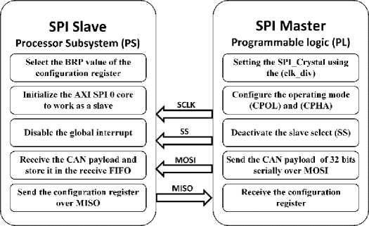
Fig. 3. SPI Block Diagram
-
A. SPI Master
The SPI master was implemented in the programmable logic of ZedBoard using the VHDL code. To begin the communication process, the master should first configure the SPI clock (SCLK) with a frequency less than or equal to the maximum frequency of the slave side. The SCLK was derived from the external clock source called (SPI_Crystal) in the processor side. To adjust the value of the SCLK that was
configured within 1 MHz in the processor system, the SPI_ Crystal could be divided by an integer number called (clk_div).
In addition to the setting of the SCLK which was responsible for the synchronization of the data communication, the master should also configure the operating mode. The configuration was done through the clock polarity (CPOL) and clock phase (CPHA) concerning the data to be sent. Four possible modes could be used in an SPI protocol to determine the edges of the clock signal on which the data were driven and sampled. Mode (0,1) was selected for connecting the PS to PL. In this mode, the CPOL was configured with ’0’ where the base value of the clock was zero and the CPHA was configured with ’1’ wherein the data was captured on the second clock edge (falling edge).
The operation of the SPI master was controlled by the (Enable signal) that was sent from the processor over the GPIO to prevent the SPI master for initiating the transmission till the processor is programmed. After that, the transmission was started by deactivating the slave select (SS) signal to inform the slave that the master wished to start data exchange. The signal was active low, so a low level on this line would specify the SPI master was active. After that, the data exchange of 32 bits was performed serially over MOSI and MISO between the master and the slave. Subsequently, the slave select signal was set to high logic to terminate the operation.
The information of the CAN listener had been stored in the FIFO of 96 bits line width. Each line of this FIFO was read as three separate sections. After that, every section of 32 bits was loaded to the temporary register called (data_out) which was sent serially to the slave side over MOSI.
-
B. SPI Slave
The Zynq-7000 devices included two independent SPI controllers as cores (AXI SPI 0 and AXI SPI 1). The AXI SPI 0 was configured by the C code running on the processor system to work as a slave to connect the processor with the programmable logic [23].
This slave was connected to the SPI master that was implemented in PL through the Extended Multiplexed InputOutput (EMIO).
The slave considered the transfer to begin with the first falling edge of SS. After that, the received CAN information from the master was stored again in a received FIFO which was 16 lines depth. Every 3 lines represented one CAN frame information (the first line represented the frame identifiers and some flags, where the second and the third lines represented the frame data).
It means that every 15 lines described the content of 5 CAN frames. The last line (line number 16) of the receive FIFO was filled always with dummy value that sent from the master side for display organization. This value was not considered during the read operation. If the receive FIFO was full and additional data was received, all data attempted to be written to the full receive FIFO by the SPI unit was vanished [23].
-
V. OLED
As the CAN information was transferred from the programmable logic to the processor subsystem over SPI, the final step was to display this information. The ZedBoard had an onboard display unit called Organic Light-Emitting Diode and briefly (OLED) used for digital display[6]. The OLED used the standard 12-pin connector to display CAN
information on a 128x32 pixel panel. The OLED showed the final data written on the screen until it was shut down or a new pattern is loaded to the display buffer [24].
To display the CAN information on the OLED, the following procedures were completed using the C code running on the processor system as shown in the Fig. 4:
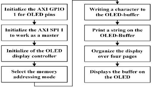
Fig. 4. OLED Display Procedures
-
A. Initialization of AXI SPI & GPIO
The OLED controller was a serial device that could be accessed using the SPI interface. The Zynq-7000 device contained two independent SPI controllers as cores (AXI SPI 0 and AXI SPI 1)[6]. The AXI SPI 1 was configured independently as a master to organize the operation of OLED as well as to send the bitmap data to the display buffer.
-
B. Initialization of Display Controller
The initialization of the OLED consisted of a sequence of operations as described in Fig. 5. The blue blocks represented the initialization of the display controller, while the gray blocks represented the configuration of display mode which was done through a series of commands.
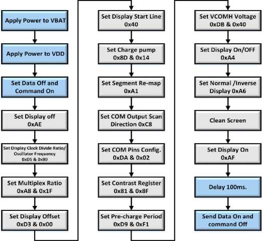
Fig. 5. Initialization Chain of OLED Controller [24]
-
C. Memory Addressing Modes
In the page addressing mode, which was used, the column address pointer was incremented automatically by 1 when a read/write operation was performed on the display RAM. If the
column address pointer arrived at the column end address position, the column address pointer was returned to the column start address. The address pointer of one page was not incremented automatically; thus, this operation should be done manually to set a new page and column addresses to access the next page RAM content [24].
The SSD1306 controller could handle 128x64 displays, but the OLED used on ZedBoard was only 128x32. For that, the display memory was organized as 4 pages of 128 columns each. All characters on the OLED were represented with 8x8 bit (pixel).
-
D. Write a Character to the OLED-Buffer
The operation of writing a character to the OLED-buffer was performed by using the character column number and row number to determine the cursor position. Equation (3) was used to create the index location for one character into the OLED buffer:
Index = (X * 8) + (Y * 16 ∙ (3)
Where X represented the x position and Y represented the y position for the character location. The bitmap style fonts were stored in the display pattern, where one bit represented one pixel of information to be displayed (monochrome font).
-
E. Print a String on the OLED-Buffer
As CAN information should be displayed in a string format, the operation of writing a character to the buffer must be repeated during the display. The OLED could show 16 characters on each page simultaneously; therefore, the writing character function had to be repeated 16 times for each page.
-
F. OLED Display Organization
The display on the OLED was organized in a way where the first page of the screen showed the string ("ID.REMOT.IDE.EID.CRC"). This string described the content of the next page (second page) which contains the value of the standard identifier, the value of the remote frame flag, the value of extended identifier and finally the value of the CRC result flag. The third page showed the string (“CAN DATA FRAME”). This string described the content of the fourth page which contains the CAN data field information (RX_Data).
-
A. Test Requirements
To perform the test for the implemented CAN listener controller, several components and software were utilized to provide the complete environment for the CAN network as follows:
-
• CAN Transceiver: In general, each node in the CAN network should have a device that worked as a bridge to convert the digital signals generated by the CAN controller to differential signals that were appropriate for the transmission over the bus. It also converted the differential signals of the bus back to digital signals during the reception process [25]. The implemented 3.3-V CAN transceiver (VP235) board consisted of two ports. The RS232 port was connected to the CAN bus and the other was connected to the Pmod header of ZedBoard.
-
• CANUSB: The CANUSB was a small and low-cost dongle that provided instant CAN connectivity. This dongle could be plugged directly into any PC USB port and handled by the operating system as a standard COM Port (RS-232 serial port) which eliminated the need for any additional drivers [26].
-
• CAN Hacker: To run the CANUSB dongle and to configure its operation, software called CAN Hacker was utilized.
-
• Tera Term: was an open-source terminal emulator that supports serial port connections. It provided a connection between the host PC and the USB-UART port of ZedBoard using a USB cable. Tera Term was used to display the CAN information that was sent serially from the processor system over the USB-UART bridge chip of Zedboard.
-
B. Test Bench Setup
The procedure for creating the test bench to examine the realized CAN listener was overviewed in this section. Fig. 6, shows the structure of the network (test bench) that was used for the test.
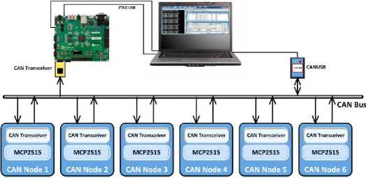
Fig. 6. Test Bench Structure
In addition to the ZedBoard and laptop computer, the test bench included six (MCP2515 CAN controller) nodes with their transceivers, CANUSB dongle, an implemented CAN transceiver and a custom-made CAN bus [27].
-
C. The Test
To test the realized CAN listener module, a series of operations were performed sequentially. The first step was achieved through setting the CAN Hacker software that was used to initialize the communication and to generate the CAN frames using the CANUSB dongle. The setting involved the selection of bit rate from the setting menu. The bit rate was configured with 50 kbps. After that, the frame identifier field was filled with 0x50F and the data field was loaded with an arbitrary payload of 8 bytes length. To make the generation of frames repeated sequentially, the period field was enabled and loaded with an appropriate value. Once the software was initialized, a sequence of frames was sent to the CAN bus using the CANUSB dongle.
Each node on the network that received the generated frames from the CANUSB dongle should respond with another frame. As a result, 7 different frames were traveled over the CAN network. To add the listener node to the network, the ZedBoard should be programmed. This was done in the SDK tool by initializing and running the processor using the .elf file, but first, the FPGA should be programmed with the bitstream that included listener design code and custom PL peripheral configuration. This process took approximately 30-60 seconds to complete, depending on the USB-JTAG traffic. After
completing the programming process, the done LED was illuminated blue and the listening process was started. Fig. 7, provided a snapshot view of the actual test operation.
In addition to the OLED that displays the received CAN information, the Tera Term software was also launched during the programming process to monitor the CAN information directly from the processor over USB-UART Bridge.
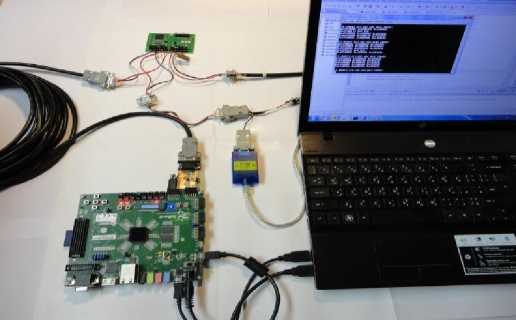
Fig. 7. Actual Test View
-
D. Test Result and Observation
Based on the above tests, the implemented CAN listener module was found to be working as expected and meets the specification required by the CAN protocol
The CAN listener controller was realized correctly on the programmable logic of ZedBoard using VHDL language. The controller could be configured to operate with different standard bit rates. The design code was divided into a sequence of processes; each one performed a specific function on the received CAN frames. No frame was sent to the CAN network since the implemented controller worked as a listener. The differential signals of CAN bus were converted to digital signals by using the implemented CAN transceiver that was connected to the ZedBoard.
The received frames were decoded correctly and saved in a temporary buffer. After that, all the received frames were accepted except those that have a bit-stuff error, CRC error or those that not match with the filter criteria. Several masks were applied accurately on the accepted frames to extract the relevant CAN information and then loaded it to the FIFO. The FIFO was implemented previously to store and retrieve the CAN information. This information was sent serially to the processor system through the SPI that was realized to connect the implemented controller with the processor system. The SPI master was well realized in the programmable logic, while the slave was implemented on the processor system.
A standalone operating system was run appropriately over the processor that enables the execution of the C code that was written to accomplish the SPI slave and to configure the operations of OLED that was used to display the obtained CAN information.
The development of the design and simulation test was performed using the Xilinx ISE WebPACK Design Suite 14 that provided the complete front-to-back design environment and held up the embedded processor design for the Zynq device. The final design of the CAN listener module was tested
properly and verified by connecting the module to the real CAN network consisting of six CAN nodes.
Finally, the processor-centric architecture for the Zynq-7000 SoC device that provided the complete processing platform and the robust combine of on-board peripherals and expansion capabilities of ZedBoard, had the fundamental role to the success this project.
-
1. HPL, S.C.J.A.R.S., Introduction to the controller area network (CAN). 2002: p. 1-17.
-
2. Di Natale, M., et al., Understanding and using the controller area network communication protocol: theory and practice. 2012: Springer Science &
Business Media.
-
3. Richards, P.J.M.T.I., A CAN physical layer discussion. 2002.
-
4. Jeganathan, N.S., A Controller Area Network Layer For Reconfigurable Embedded Systems. 2007.
-
5. Version, B.C.S., 2.0, Robert Bosch GmbH, Stuttgart, Germany, 1991.
-
6. Crockett, L.H., R.A. Elliot, and M.A. Enderwitz, The zynq book tutorials for zybo and zedboard. 2015:
Strathclyde Academic Media.
-
7. Bhutada, V., S.J. , and T.Z. , Design and Implementation of CAN Bus Controller
on FPGA. International Journal for Research in Applied Science & Engineering Technology (IJRASET), 2017. 5( XII).
-
8. Krishnamoorthy, S., Design of an ASIC chip for a Controller Area Network (CAN) protocol controller. 2006, Texas Tech University.
-
9. Katyarmal, R.D. and P.J.I.J.o.E.R. Daigavane, Design of Controller Area Network for Sensor Network Application using Verilog-HDL. 2014. 3(4).
-
10. Piao, C.-h., L. Chen, and J. Cao. A design for Controller Area Network bus real-time monitoring system. in Proceedings of 2011 International Conference on Computer Science and Network Technology. 2011. IEEE.
-
11. Abaceoae, C. and M. Postolache. Design and
Implementation of a CAN-USB Interface for Networked Embedded Systems. in 2018 22nd International
Conference on System Theory, Control and Computing (ICSTCC). 2018. IEEE.
-
12. Gong, S., et al. Design and implementation of CAN communication system based on SOPC technology. in 2017 Chinese Automation Congress (CAC). 2017.
IEEE.
-
13. Pimple, P. Sniffing the Automotive CAN Bus for Realtime Data-logging and Real Time Diagnostics Display. in 2018 International Conference on Smart Electric Drives and Power System (ICSEDPS). 2018. IEEE.
-
14. Hao, J., J. Wu, and C. Guo. Modeling and simulation of CAN network based on OPNET. in 2011 IEEE 3rd International Conference on Communication Software and Networks. 2011. IEEE.
-
15. Presi, T. Design and development Of PIC microcontroller based vehicle monitoring system using Controller Area Network (CAN) protocol. in 2013 International Conference on Information
Communication and Embedded Systems (ICICES). 2013. IEEE.
-
16. Singh, V.K., K.J.I.J.o.E.T. Archana, and Technology, Implementation of CAN Protocol in Automobiles Using Advanced Embedded System. 2013. 4: p. 4422-4427.
-
17. Shinde, A.S. and V.B. Dharmadhikari, Controller area network for vehicle automation. 2012.
-
18. Al-Mekkawy, M.K., et al. Reliable design of the CAN bit synchronization block. in Proceedings of the WSEAS Conference: Information Science,
Communications and Applications (ISCA 2005). 2005.
-
19. Watterson, C.J.A.N.A.-., Analog Devices, Inc, Controller area network (CAN) implementation guide. 2012.
-
20. Voss, W., A comprehensible guide to controller area network. 2008: Copperhill Media.
-
21. Specification, C., 2.0, Part-A and Part-B. CAN in Automation (CiA), Am Weichselgarten 26, D-91058 Erlangen. 2002.
-
22. Shingare, T.D., R.J.I.J.o.I.T. Patil, and E. Engineering, SPI implementation on fpga. 2013. 2(2): p. 7-9.
-
23. XILINX, LogiCORE IP AXI Serial Peripheral Interface (AXI SPI) (v1.02.a). 2012.
-
24. SYSTECH, S., OLED/PLED Segment/Common Driver with Controller in SSD1306 2008.
-
25. MCP–High-speed, C.J.M.T.I., Transceiver Data sheet.
2003.
-
26. LAWICEL, CANUSB Manual. 2011: Sweden.
-
27. Fink, A. and H. Beikirch. Radio-based human tracking for large indoor environments using distributed centroid location estimation. in 2013 IEEE 7th
International Conference on Intelligent Data Acquisition and Advanced Computing Systems
(IDAACS). 2013. IEEE.
Discussion and feedback