PREPARATION AND CHARACTERIZATION OF PbSe THIN FILMS BY CHEMICAL BATH DEPOSITION
on
ISSN 1907-9850
PREPARATION AND CHARACTERIZATION OF PbSe THIN FILMS BY CHEMICAL BATH DEPOSITION
Anuar Kassim*a, Tan Wee Teea, Dzulkefly Kuang Abdullaha, Md. Jelas Harona, Ho Soon Mina, Shanthi Monohorna and Saravanan Nagalingamb
aDepartment of Chemistry, Faculty of Science, Universiti Putra Malaysia, 43400 Serdang, Selangor, Malaysia;
bDepartment of Bioscience and Chemistry, Faculty of Engineering and Science, Universiti Tunku Abdul Rahman, 53300 Kuala Lumpur, Malaysia
*Corresponding author. Tel: 603-89466779; Email: anuar@science.upm.edu.my
ABSTRACT
PbSe thin films were grown onto glass substrates by chemical bath deposition method. Structure and surface morphology of thin films were characterized by X-ray diffraction and scanning electron microscopy. The band gap energy and type of optical transition were determined from optical absorbance data. The deposition parameters were optimized to obtain good quality of thin films. X-ray diffraction indicates that the films have cubic structure. The SEM micrograph showed the films do not cover the glass substrate completely and consisted of irregular shaped grains. The films show good optical properties with high absorption in the visible region and the band gap value was estimated to be 1.3 eV.
Keywords : Chemical bath deposition, Lead selenide, X-ray diffraction, thin films.
INTRODUCTION
The PbSe thin films attract attention of many researchers because they are cheap, abundant and they posses semiconducting properties. In the past, several techniques such as electrodeposition (Molin and Dikusar, 1995), chemical bath deposition (Grozdanov et al., 1999), electrochemical atomic layer epitaxy (Vaidyanathan et al., 2004), photochemical (Zhu et al., 2001), molecular beam epitaxy (Gautier et al., 1998) and pulsed laser deposition (Rumianowski et al., 2003) method have been used in the deposition of PbSe thin films. In recent years, the semiconductors thin films have received widespread interest in the field of solar cells (Ristov et al., 2001; Messina et al., 2007; Anuar et al., 2008), optoelectronic devices, photoconductors, sensor and infrared detector devices. Every technique of thin film deposition
has its own advantages and disadvantages. But the technique such as chemical bath deposition, which is simple, no requirement of sophisticated instruments, minimum material wastage and economical way of large area deposition is of interest to researchers. Up-to-date, chemical bath deposition method has been successfully used to deposit many different semiconductors thin films including PbS (Larramendi et al., 2001), ZnS (Ubale et al., 2007), MnS (Gumus et al., 2007), CdS (Li et al., 2005), Cd1-xZnxS (Gaewdang and Gaewdang, 2005) and CuBiS2 (Sonawane et al., 2004).
In this work, PbSe thin film has been chemically deposited on glass substrate from an aqueous solution containing lead nitrate and sodium selenate. The triethanolamine is used as a complexing agent during deposition. The deposition parameters were optimized to obtain good quality thin films. The structure of the film
was measured by X-ray diffraction technique. The morphology and optical absorption properties were determined by using scanning electron microscopy and UV-Vis spectrophotometer, respectively.
MATERIALS AND METHOD
All the chemicals used for the deposition were analytical grade. It includes lead nitrate [Pb(NO3)2], sodium selenate [Na2O4Se], triethanolamine [(HOC2H4)3N] and hydrochloric acid [HCl]. All the solutions were prepared in deionised water (Alpha-Q Millipore). During the deposition, the triethanolamine (TEA) is used as a complexing agent while lead nitrate and sodium selenate act as a source of lead and selenide ion, respectively.
The glass substrates of the dimension of 25.4 mm x 76.2 mm x 1 mm were degreased in ethanol for 10 min and then ultrasonically cleaned with distilled water for another 15 min before deposition of films. Deposition of PbSe thin film was carried out using following procedure: 20 ml of 0.15 M lead nitrate solution was taken in a 100 mL beaker. Then, 10 mL of triethanolamine solution was added in the reaction bath. Following that, 20 mL of 0.15 M sodium selenate solution was added into the mixture. By adding drop-wise hydrochloric acid solution, the pH of resultant solution was adjusted to 6. The beaker containing resultant solution was kept in water bath. The temperature of the bath was then allowed to increase slowly up to 80 °C. The clean microscope glass slides were placed in the bath, supported vertically on the wall of the beaker. After 60 min, the glass slide was removed, washed several times with distilled water, dried naturally in desiccators for further characterization.
In order to investigate the crystallographic properties of the PbSe thin films, we carried out the X-ray diffraction (XRD) analysis using Philips PM 11730 diffractometer with CuKα (λ=1.5418 Å)
radiation. The surface morphology was observed by a scanning electron microscopy (JEOL, JSM-6400). The optical absorption measurement was carried out in the wavelength range from 350 to 800 nm using a Perkin Elmer UV/Vis Lambda 20 Spectrophotometer. The film-coated glass substrate was placed across the sample radiation pathway while the uncoated glass substrate was put across the reference path. The absorption data were manipulated for the determination of the band gap energy.
RESULTS AND DISCUSSION
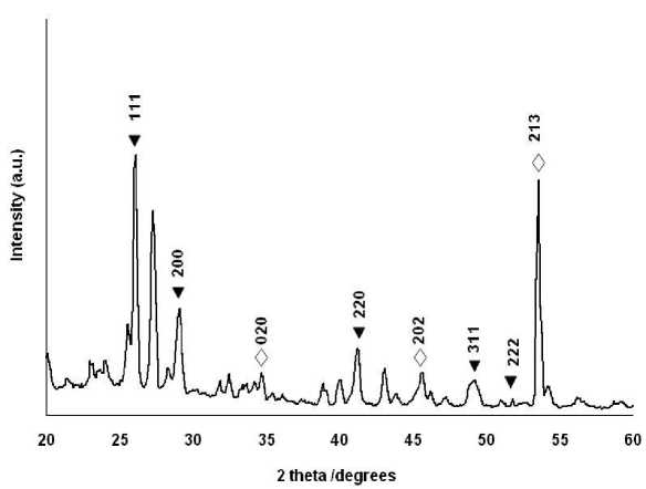
The X-ray diffraction pattern of film deposited at optimized deposition parameters is shown in Figure 1. The observed d-spacing and the respective prominent peaks correspond to reflection from the (111), (200), (220), (311) and (222) planes, which coincide well with the JCPDS data (reference No.: 00-065-1040). Therefore, it has been concluded that the deposited PbSe thin films are polycrystalline in nature with cubic structure. The lattice parameters of the cubic structure are equal to a = 6.128 Å, b = 6.128 Å and c = 6.128 Å. On the other hand, the appearance of three other peaks attributable to silicon oxide (JCPDS reference No.: 01-074-0201) at 2θ = 34.5°, 45.3° and 53.9° with interplanar distances of 2.56, 2.06 and 1.69 Å, respectively also could be detected. The presence of silicon oxide (SiO2) comes from the substrates during deposition process.
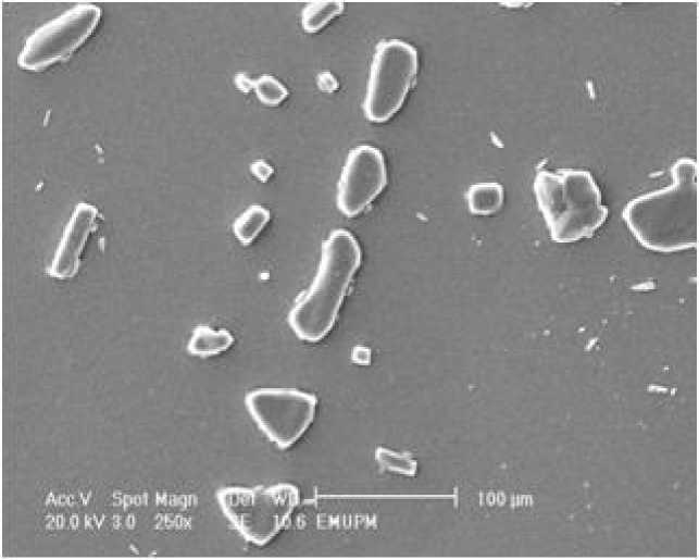
Scanning electron microscopy (SEM) was used to reveal the microstructure of the films. Figure 2 shows the SEM micrograph of lead selenide thin film deposited under optimized parameters at 250x magnification. Clearly, the films do not cover the glass substrate completely, as could be observed in SEM micrograph. The deposits have formed grains of various sizes ranging from 20 to 50 μm.

Fig. 1. X-ray diffraction pattern of FeS2 thin films deposited at optimized parameters ( VPbSe, ◊ SiO2)

Fig. 2. The SEM micrograph of PbSe thin films deposited at optimized parameters
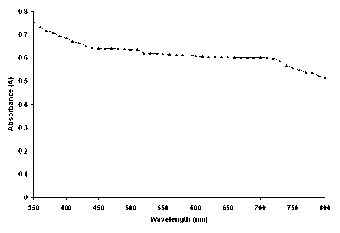
The optical properties of the films deposited on glass substrates were investigated from the absorbance measurement in the range of 350-800 nm. Figure 3 shows the absorbance spectrum for PbSe thin film deposited at
optimized deposition conditions. This spectrum shows a gradually increasing absorption throughout the visible region which makes it possible for this material to be used in a photoelectrochemical cells.

Fig. 3. Optical absorbance versus wavelength of PbSe thin films deposited at optimized parameters

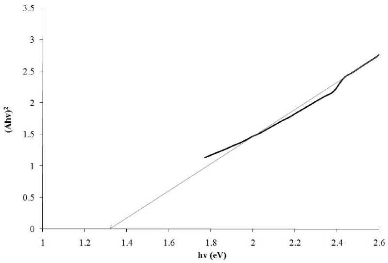
Fig. 4. Plot of (Ahv)2 versus hv of PbSe thin films deposited at optimized parameters
Band gap energy and transition type can be derived from mathematical treatment of data obtained from optical absorbance versus wavelength with Stern relationship of near-edge absorption (Equation 1):
[k(hv - Eg)n/2] A = ------„ --- (1)
hv
where v is the frequency, h is the Planck’s constant, k equals a constant while n carries the value of either 1 or 4. The value of n is 1 and 4 for the direct transition and indirect transition, respectively. The band gap of the film was calculated by plotting (Ahv)2 against hv shown in Figure 4. The linear nature of the plot indicated the existence of direct transition. The band gap was obtained from extrapolating the straight portion of the graph on the hv axis at (Ahv)2/n = 0. The direct band gap value is found to be 1.3 eV.
CONCLUSIONS
The PbSe thin films have been prepared by the chemical bath deposition technique under optimized deposition conditions. Deposition was carried out from aqueous solutions using lead nitrate and sodium selenate as Pb2+ and Se2- ion source, respectively. The thin films produced were polycrystalline and have a cubic structure. The SEM micrograph showed the films do not cover the glass substrate completely and consisted of irregular shaped grains. The PbSe thin films exhibited direct band gap transition with band gap energy of 1.3 eV.
ACKNOWLEDGEMENTS
The authors would like to thank the Department of Chemistry, Universiti Putra Malaysia for the provision of laboratory facilities and MOSTI for the National Science Fellowship (NSF).
REFERENCES
Anuar, K., Ho, S.M., Tan, W.T., Atan, S., Zulkefly, K., Md. Jelas, H., and Saravanan, N., 2008, Cathodic
Electrodeposition of Chalcogenide Thin Films Cu4SnS4 for Solar Cells, Chiang Mai J. Sci. Technol., 7 : 317-326
Gaewdang, N., and Gaewdang, T., 2005, Investigations on chemically deposited Cd1-xZnxS thin films with low Zn content, Mater. Lett., 59: 3577-3584
Gautier, C., Breton, G., Nouaoura, M., Cambon, M., Charar, S., and Averous, M. 1998, Sulfide films on PbSe thin layer grown by MBE, Thin Solid Films, 315: 118-122
Grozdanov, I., Najdoski, M., and Dey, S.K., 1999, A simple solution growth technique for PbSe thin films, Mater. Lett., 38: 28-32
Gumus, C., Ulutas, C., and Ufuktepe, Y., 2007, Optical and structural properties of manganese sulfide thin films, Opt. Mater., 29: 1183-1187
Larramendi, E.M., Calzadilla, O., Arias, A.G., Hernandez, E., and Garcia, J.R., 2001, Effect of surface structure on photosensitivity in chemically deposited PbS thin films, Thin Solid Films, 389: 301-306
Li, W.Y., Cai, X., Chen, Q.L., and Zhou, Z.B., 2005, Influence of growth process on the structural, optical and electrical properties of CBD-CdS films, Mater. Lett., 59: 1-5
Messina, S., Nair, M.T.S., and Nair, P.K., 2007, Antimony sulfide thin films in chemically dddeposited thin film photovoltaic cells, Thin Solid Films, 515: 5777-5782
Molin, A.N., and Dikusar, A.I., 1995,
Electrochemical deposition of PbSe thin films from aqueous solutions, Thin Solid Films, 265: 3-9
Ristov, M., Sinadinovski, G., Mitreski, M., and Ristova, M., 2001, Photovoltaic cells based on chemically deposited p-type SnS, Sol. Energy Mater. Sol. Cells, 69: 17-24
Rumianowski, R.T., Dygdala, R.S., Jung, W. and Bala, W., 2003, Growth of PbSe thin films on Si substrates by pulsed laser deposition method, J. Cryst. Growth, 252: 230-235
Sonawane, P.S., Wani, P.A., Patil, L.A., and Seth, T., 2004, Growth of CuBiS2 thin films by chemical bath deposition technique from and acidic bath, Mater. Chem. Phys., 84: 221-227
Ubale, A.U., Sangawar, V.S., and Kulkarni, D.K., 2007, Size dependent optical characteristics of chemically deposited
nanostructured ZnS thin films, Bull. Mater. Sci., 30: 147-151
Vaidyanathan, R., Stickney, J.L., and Happek, U., 2004, Quantum confinement in PbSe thin films electrodeposited by electrochemical atomic layer epitaxy (EC-ALE), Electrochim. Acta, 49: 1321– 1326
Zhu, J.J., Liao, X.H., Wang, J., and Chen, H.Y. 2001, Photochemical synthesis and characterization of PbSe nanoparticles, Mater. Res. Bull., 36: 1169–1176
6
Discussion and feedback